Table Of Content

Cable & Wire HarnessCreate, manage, and document your cable and wire harness assemblies in a comprehensive, integrated platform. Simulation & AnalysisTest and optimize before you build with our array of best-in-class simulation and virtual prototyping solutions. Synopsys helps you protect your bottom line by building trust in your software—at the speed your business demands.
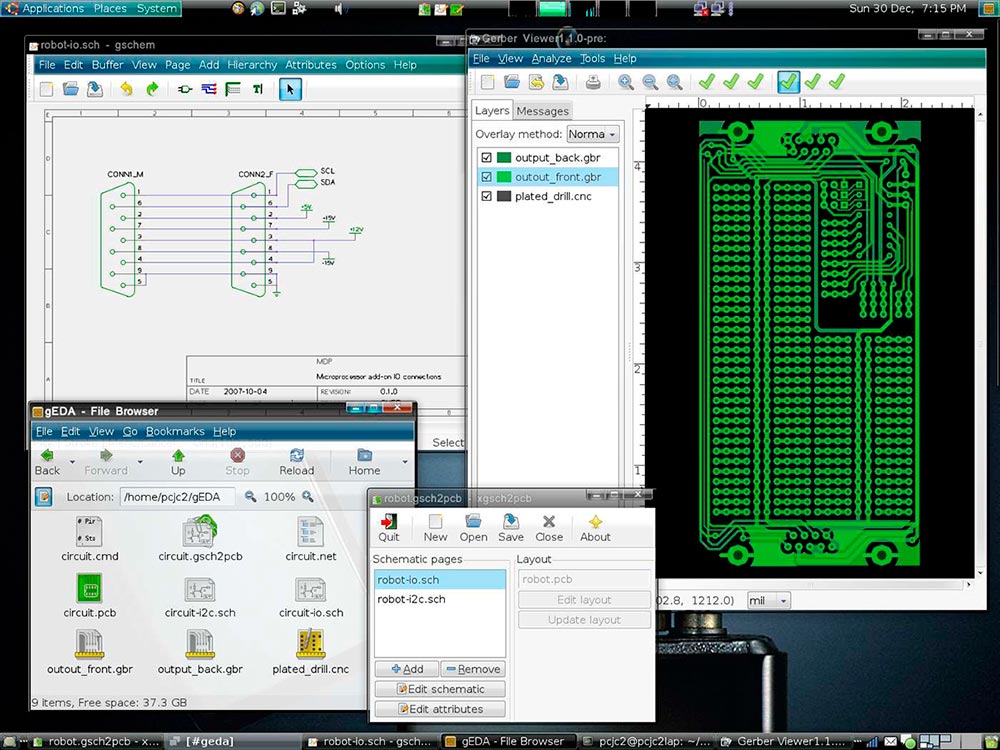
PCB Electronic Design Automation Tools
The three primary companies leading this phase were Applicon, Calma, and Computervision. It is interesting to note that in these early days Calma developed a format to represent IC layouts called GDS, named after its product, Graphic Design System. The GDS II version of this format continued to be used as the de-facto format to communicate IC layout information for decades.
The Importance of Electronic Design Automation in a Technology-Driven World
The specific procedure entails such steps as wiring, signal integrity analysis, parasitic parameter extraction, unit layout and optimisation, clock tree synthesis (CTS), layout physical planning, power analysis, and physical verification. While EDA solutions are not directly involved in the manufacture of chips, they play a critical role in three ways. First, EDA tools are used to design and validate the semiconductor manufacturing process to ensure it delivers the required performance and density.
What are the leading companies in the EDA industry?
Verification can also take the form of comparing the implemented circuit to the original description to ensure it faithfully reflects the required function. Functional verification of a chip can also use simulation technology to compare actual behavior to expected behavior. These approaches are limited by the completeness of the input stimulus provided. Another approach is to verify the behavior of the circuit algorithmically, without the need for input stimulus.
Electronic System Design Industry Posts Record $4.7B in Revenue in Q3 2023, ESD Alliance Reports - HPCwire
Electronic System Design Industry Posts Record $4.7B in Revenue in Q3 2023, ESD Alliance Reports.
Posted: Mon, 08 Jan 2024 08:00:00 GMT [source]
Contrary to formal verification, simulation-based verification usually cannot ensure complete correctness in the design. Instead, the design is put under a test bench with certain random or fixed-pattern input stimuli applied, while the outputs are compared to the reference outputs to verify if the design’s behavior is expected. While simulation is the bread and butter of functional verification, simulation-based verification can also suffer from long verification times. It is not uncommon for the verification of a complex design to take weeks to complete. The implementation and flow of processes are mostly considered in the layout and simulation phases of the back-end design of digital circuits.
In our recent IP Lifecycle Management for Chiplet-Based SoCs webinar, Helix IPLM founder Simon Butler walks through best practices for managing IPs from inception through SoC integration. With traceability in mind, every aspect of the IP lifecycle is visible in Helix IPLM in easy-to-understand, configurable dashboards. Designers can see the projects the IP has been used in, any outstanding bugs, derivative designs, regression status, and much more.
What Are EDA Tools?
Something rather significant happened during this time – the commercial application-specific integrated circuit, or ASIC, industry was also born. With the emergence of the ASIC industry, the custom chips that were previously reserved for the very large system OEMs were now within reach of many more design teams. With this new market, the need for tools to automate the simulation, design, and verification of chips became far more widespread. A lot of the internal, captive teams at the large OEMs found new, exciting, and lucrative work in this new market and so the commercial EDA industry began to grow.
Making eco-friendly microelectronics ASU News - ASU News Now
Making eco-friendly microelectronics ASU News.
Posted: Thu, 16 Nov 2023 08:00:00 GMT [source]
Widely used were the Espresso heuristic logic minimizer,[6] responsible for circuit complexity reductions and Magic,[7] a computer-aided design platform. Another crucial development was the formation of MOSIS,[8] a consortium of universities and fabricators that developed an inexpensive way to train student chip designers by producing real integrated circuits. The basic concept was to use reliable, low-cost, relatively low-technology IC processes and pack a large number of projects per wafer, with several copies of chips from each project remaining preserved.
China's domestic EDA market share doubled, thanks to support from 3,451 local IC design firms
The 61st DAC will be held in June 2024 at the Moscone West Center in San Francisco, CA. As a design engineer in the electronic design ecosystem, I attend DAC to find the latest solutions and methodologies in AI, EDA, chip verification, design, and more. The technical program provides education for me and my colleagues, while the exhibits allow for firsthand interaction with vendors. The DAC conference draws over 5,000 attendees that allows me to meet and collaborate with other designers in the ecosystem.
Harry Foster is Chief Scientist Verification for Siemens Digital Industries Software; and is the Co-Founder and Executive Editor for the Verification Academy. Foster served as the 2021 Design Automation Conference General Chair and is currently serving as Past Chair. He holds multiple patents in verification and has co-authored six books on verification.
Overall, EDA tools are crucial in improving design efficiency, reducing time-to-market, enhancing design quality, and enabling the development of complex electronic systems. As designs have grown increasingly complicated, EDA software has become very important for developers involved in the production of printed circuit boards (PCB) and other circuit boards. If something goes wrong in the design process, electricity may not flow through the circuit correctly, rendering it dysfunctional.
Examples of simulation electronic design automation technology include sophisticated, high-speed prototyping. Simulation EDA tools remove the trial and error of semiconductor design, which can have catastrophic costs. Where chips contained thousands of transistors in the 1970s, they have more than a hundred billion today, and it’s impossible to create these designs manually. It’s a category of tools that help electrical engineers design and develop ever more complex chips.

No comments:
Post a Comment